D Flip Flop Schematic
Vhdl tutorial 16: design a d flip-flop using vhdl Flop proposed tspc Flop flops jk eee adbu logic retains
D Flip Flop [Explained] In Detail - EEE PROJECTS
Eee world, department of eee, adbu: digital flip-flops – sr, d, jk and D flip flop [explained] in detail Flip flop explained electronics general
Flip flop circuit logic explained delay detail
D flip flop explained in detailFlip flop vhdl using truth table tutorial circuit Cmos d flip flop circuit designFlop cmos electrical.
Flop flip schematic pmos nmos inverters parallel vertically combinationEe 421l, fall 2018, lab project 1 proposed d-ff circuit schematic of proposed d flip-flop is as shown.

VHDL Tutorial 16: Design a D flip-flop using VHDL
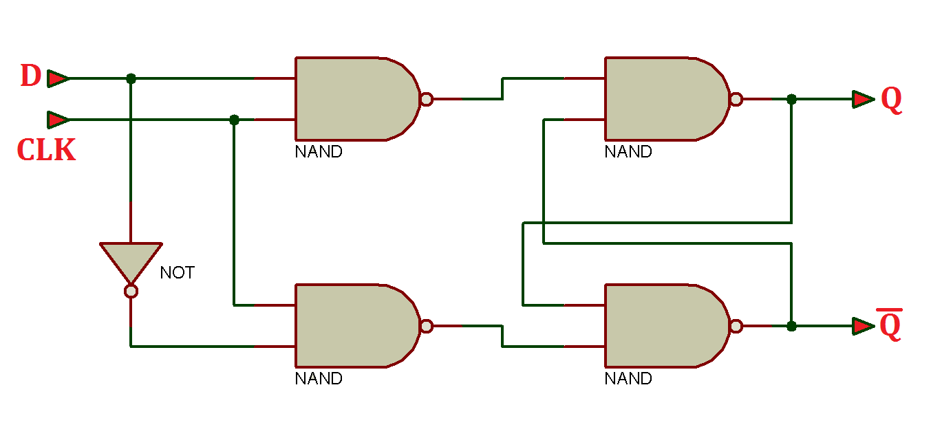
![D Flip Flop [Explained] In Detail - EEE PROJECTS](https://i2.wp.com/eeeproject.com/wp-content/uploads/2017/09/D-flip-flop-logic-circuit.jpg)
D Flip Flop [Explained] In Detail - EEE PROJECTS

EEE World, Department of EEE, ADBU: Digital Flip-Flops – SR, D, JK and

Cmos D Flip Flop Circuit Design

1 Proposed D-ff Circuit schematic of proposed D flip-flop is as shown

EE 421L, Fall 2018, Lab Project